
1
HV220/HV20220/HV20320
A011705
D
LE
CL
LE
CL
D
LE
CL
D
LE
CL
D
LE
CL
D
LE
CL
D
LE
CL
D
LE
CL
D
LE
CL
8 BIT
SHIFT
REGISTER
LEVEL
SHIFTERS
OUTPUT
SWITCHES
LATCHES
SW0
SW1
SW2
SW3
SW4
SW5
SW6
SW7
V
PP
V
NN
V
DD
D
OUT
D
IN
CLK
Low Charge Injection
8-Channel High Voltage Analog Switches
Features
HVCMOS
�
technology for high performance
Very low quiescent power dissipation � 10
�
A
Output on-resistance typically 22 ohms
Low parasitic capacitances
DC to 10MHz analog signal frequency
-60dB typical output off isolation at 5MHz
CMOS logic circuitry for low power
Excellent noise immunity
On-chip shift register, latch and clear logic circuitry
Flexible high voltage supplies
Block Diagram
HV220/HV20220/HV20320
Applications
Medical ultrasound imaging
Piezoelectric transducer drivers
General Description
These devices are low charge injection 8-channel high-voltage
analog switch integrated circuits (ICs) intended for use in
applications requiring high voltage switching controlled by low
voltage control signals, such as ultrasound imaging and print-
ers. Input data is shifted into an 8-bit shift register which can
then be retained in an 8-bit latch. To reduce any possible clock
feed-through noise, Latch Enable Bar (LE) should be left high
until all bits are clocked in. Using HVCMOS technology, these
switches combine high voltage bilateral DMOS switches and
low power CMOS logic to provide efficient control of high voltage
analog signals.
These ICs are suitable for various combinations of high voltage
supplies, e.g., V
PP
/V
NN
: +50V/�150V, or +100V/�100V.B
B021706

2
HV220/HV20220/HV20320
B021706
Symbol
Parameter
Value
V
DD
Logic power supply voltage
1, 3
4.5V to 13.2V
V
PP
Positive high voltage supply
1, 3
40V to V
NN
+ 200V
V
NN
Negative high voltage supply
1, 3
-40V to -160V
V
IH
High-level input voltage
V
DD
-1.5V to V
DD
V
IL
Low-level input voltage
0V to 1.5V
V
SIG
Analog signal voltage peak to peak
V
NN
+10V to V
PP
-10V
2
T
A
Operating free air-temperature
0�C to 70�C
Notes:
1 Power up/down sequence is arbitrary except GND must be powered-up first and powered-down last.
2 V
SIG
must be V
NN
V
SIG
V
PP
or floating during power up/down transition.
3 Rise and fall times of power supplies V
DD
, V
PP
, and V
NN
should not be less than 1.0msec.
Operating Conditions
Ordering Information
Absolute Maximum Ratings*
V
DD
Logic power supply voltage
-0.5V to +15V
V
PP
- V
NN
Supply voltage
220V
V
PP
Positive high voltage supply
-0.5V to V
NN
+200V
V
NN
Negative high voltage supply
+0.5V to -200V
Logic input voltages
-0.5V to V
DD
+0.3V
Analog Signal Range
V
NN
to V
PP
Peak analog signal current/channel
3.0A
Storage temperature
-65�C to +150�C
Power dissipation:
28-Lead
PLCC
1.2W
48-Lead
TQFP
1.0W
26-Lead
BCC
1.0W
25-Lead
FPBGA
1.0W
*
Absolute Maximum Ratings are those values beyond which damage to
the device may occur. Functional operation under these conditions is not
implied. Continuous operation of the device at the absolute rating level
may affect device reliability. All voltages are referenced to device ground.
Package Options
Device
28-Lead PLCC
48-Lead TQFP
26-Lead BCC
25-Lead FPBGA
HV20220
HV20220PJ
HV20220FG
-
-
HV20220PJ-G
HV20220FG-G
HV20320
HV20320PJ
-
-
-
HV20320PJ-G
HV220
-
-
-
HV220GA
HV220B1-G
HV220GA-G
-G indicates the part is RoHS compliant (Green)

3
HV220/HV20220/HV20320
B021706
Notes:
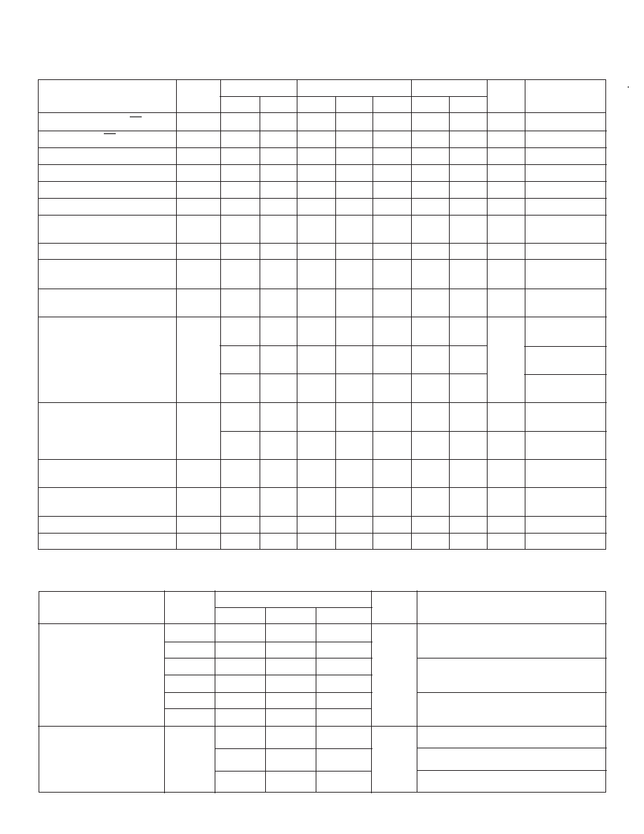
1. The eight switches operate independently.
2. Serial data is clocked in on the L
to
H transition CLK.
3. The switches go to a state retaining their present condition at the rising edge of LE. When LE is low the shift register
data flows through the latch.
4. D
OUT
is high when data in shift register 7 is high.
5. Shift register clocking has no effect on the switch states if LE is H.
6. The clear input overrides all other inputs.
D0
D1 D2 D3
D4
D5 D6 D7
LE
CL
SW0 SW1 SW2 SW3 SW4 SW5 SW6 SW7
L
L
L
OFF
H
L
L
ON
L
L
L
OFF
H
L
L
ON
L
L
L
OFF
H
L
L
ON
L
L
L
OFF
H
L
L
ON
L
L
L
OFF
H
L
L
ON
L
L
L
OFF
H
L
L
ON
L
L
L
OFF
H
L
L
ON
L
L
L
OFF
H
L
L
ON
X
X
X
X
X
X
X
X
H
L
HOLD PREVIOUS STATE
X
X
X
X
X
X
X
X
X
H
OFF OFF OFF OFF OFF OFF OFF OFF
Truth Table

4
HV220/HV20220/HV20320
B021706
Electrical Characteristics
DC Characteristics
(over recommended operating conditions unless otherwise noted)
30
26
38
48
I
SIG
= 5mA
V
PP
= 40V,
25
22
27
32
I
SIG
= 200mA V
NN
= -160V
Small Signal Switch (ON)
R
ONS
25
22
27
30
ohms
I
SIG
= 5mA
V
PP
= 100V,
Resistance
18
18
24
27
I
SIG
= 200mA V
NN
= -100V
23
20
25
30
I
SIG
= 5mA
V
PP
= 160V,
22
16
25
27
I
SIG
= 200mA V
NN
= -40V
Small Signal Switch (ON)
R
ONS
20
5.0
20
20
%
I
SW
= 5mA, V
PP
= 100V,
Resistance Matching
V
NN
= -100V
Large Signal Switch (ON)
R
ONL
15
ohms
V
SIG
= V
PP
- 10V, I
SIG
= 1A
Resistance
Switch Off Leakage
I
SOL
5.0
1.0
10
15
�A
V
SIG
= V
PP
- 10V
Per Switch
and V
NN
+10V
DC Offset Switch Off
300
100
300
300
mV
R
L
= 100
DC Offset Switch On
500
100
500
500
mV
R
L
= 100K
Pos. HV Supply Current
I
PPQ
10
50
�A
ALL SWs OFF
Neg. HV Supply Current
I
NNQ
-10
-50
�A
ALL SWs OFF
Pos. HV Supply Current
I
PPQ
10
50
�A
ALL SWs ON I
SW
= 5mA
Neg. HV Supply Current
I
NNQ
-10
-50
�A
ALL SWs ON I
SW
= 5mA
Switch Output
3.0
3.0
2.0
2.0
A
V
SIG
duty cycle
0.1%
Peak Current
Output Switch Frequency
f
SW
50
KHz
Duty Cycle = 50%
6.5
7.0
8.0
V
PP
= 40V,
V
NN
= -160V
I
PP
Supply Current
I
PP
4.0
5.0
5.5
mA
V
PP
= 100V,
V
NN
= -100V
4.0
5.0
5.5
V
PP
= 160V,
V
NN
= -40V
6.5
7.0
8.0
V
PP
= 40V,
V
NN
= -160V
I
NN
Supply Current
I
NN
4.0
5.0
5.5
mA
V
PP
= 100V,
V
NN
= -100V
4.0
5.0
5.5
V
PP
= 160V,
V
NN
= -40V
Logic Supply
I
DD
4.0
4.0
4.0
mA
f
CLK
= 5MHz, V
DD
= 5.0V
Average Current
Logic Supply
I
DDQ
10
10
10
�A
Quiescent Current
Data Out Source Current
I
SOR
0.45
0.45
0.70
0.40
mA
V
OUT
= V
DD
- 0.7V
Data Out Sink Current
I
SINK
0.45
0.45
0.70
0.40
mA
V
OUT
= 0.7V
Logic Input Capacitance
C
IN
10
10
10
pF
0�C
+25�C
+70�C
Characteristics
Sym
Units
Test Conditions
min
max
min
typ*
max
min
max
50KHz
Output
Switching
Frequency
with no
load
*
Typical values are only for HV202/HV203
5
HV220/HV20220/HV20320
B021706
AC Characteristics
(over operating conditions V
DD
= 5V, unless otherwise noted)
+25�C Units
Characteristics Sym
Test Conditions
min typ* max
Electrical Characteristics
Electrical Characteristics
AC Characteristics
(over operating conditions V
DD
= 5V, unless otherwise noted)
0�C
+25�C
+70�C
Characteristics
Sym
min
max
min
typ*
max
min
max
Units
Test Conditions
Set Up Time Before LE Rises
t
SD
150
150
150
ns
Time Width of LE
t
WLE
150
150
150
ns
Clock Delay Time to Data Out
t
DO
150
150
150
ns
Time Width of CL
t
WCL
150
150
150
ns
Set Up Time Data to Clock
t
SU
15
15
8.0
20
ns
Hold Time Data from Clock
t
h
35
35
35
ns
Clock Freq
f
CLK
5.0
5.0
5.0
MHz
50% duty cycle
f
DATA
= f
CLK
/2
Clock Rise and Fall Times
t
r
, t
f
50
50
50
ns
Turn On Time
t
ON
5.0
5.0
5.0
�s
V
SIG
= V
PP
-10V,
R
L
= 10K
Turn Off Time
t
OFF
5.0
5.0
5.0
�s
V
SIG
= V
PP
-10V,
R
L
= 10K
20
20
20
V
PP
= 160V,
V
NN
= -40V
Maximum V
SIG
Slew Rate
dv/dt
20
20
20
V/ns
V
PP
= 100V,
V
NN
= -100V
20
20
20
V
PP
= 40V,
V
NN
= -160V
Off Isolation
KO
-30
-30
-33
-30
dB
f = 5MHz,
1K
//15pF load
-58
-58
-58
dB
f = 5MHz,
50
load
Switch Crosstalk
K
CR
-60
-60
-70
-60
dB
f = 5MHz,
50
load
Output Switch Isolation
I
ID
300
300
300
mA
300ns pulse width,
Diode Current
2.0% duty cycle
Off Capacitance SW to GND
C
SG(OFF)
5.0
17
5.0
12
17
5.0
17
pF
0V, 1MHz
On Capacitance SW to GND
C
SG(ON)
25
50
25
38
50
25
50
pF
0V, 1MHz
Output Voltage Spike
+V
SPK
150
V
PP
= 40V, V
NN
= -160V, R
L
= 50
� V
SPK
150
+V
SPK
150
V
PP
= 100V, V
NN
= -100V, R
L
= 50
� V
SPK
150
mV
+V
SPK
150
V
PP
= 160V, V
NN
= -40V, R
L
= 50
� V
SPK
150
Charge Injection
820
V
PP
= 40V, V
NN
= -160V, V
SIG
= 0V
Q
600
pC
V
PP
= 100V, V
NN
= -100V, V
SIG
= 0V
350
V
PP
= 160V, V
NN
= -40V, V
SIG
= 0V
*
Typical values are only for HV202/HV203

6
HV220/HV20220/HV20320
B021706
Test Circuits
Switch OFF Leakage
I
SOL
V
PP
5V
V
NN
V
PP
V
NN
V
DD
GND
V
NN
+10V
V
PP
-10V
DC Offset ON/OFF
V
PP
5V
V
NN
V
PP
V
NN
V
DD
GND
V
OUT
100K
R
L
T
ON
/T
OFF
Test Circuit
V
PP
5V
V
NN
V
PP
V
NN
V
DD
GND
V
PP
-10V
R
L
10K
V
OUT
Isolation Diode Current
I
ID
V
PP
5V
V
NN
V
PP
V
NN
V
DD
GND
V
NN
V
SIG
Crosstalk
K
CR
= 20Log
V
OUT
V
IN
V
IN
= 10 V
P-P
@5MHz
NC
50
V
PP
5V
V
NN
V
PP
V
NN
V
DD
GND
50
Charge Injection
V
PP
5V
V
NN
V
PP
V
NN
V
DD
GND
V
SIG
V
OUT
1000pF
Q = 1000pF x V
OUT
V
OUT
Output Voltage Spike
V
PP
5V
V
NN
V
PP
V
NN
V
DD
GND
V
OUT
1K
R
L
50
+V
SPK
-V
SPK
OFF Isolation
K
O
= 20Log
V
OUT
V
IN
V
IN
= 10 V
P-P
@5MHz
V
PP
5V
V
NN
V
PP
V
NN
V
DD
GND
R
L
V
OUT

7
HV220/HV20220/HV20320
B021706
Logic Timing Waveforms
Block Diagram
D
LE
CL
LE
CL
D
LE
CL
D
LE
CL
D
LE
CL
D
LE
CL
D
LE
CL
D
LE
CL
D
LE
CL
8 BIT
SHIFT
REGISTER
LEVEL
SHIFTERS
OUTPUT
SWITCHES
LATCHES
SW0
SW1
SW2
SW3
SW4
SW5
SW6
SW7
V
PP
V
NN
V
DD
D
OUT
D
IN
CLK
DATA
IN
CLOCK
DATA
OUT
D
N - 1
N
N + 1
D
D
50%
50%
50%
50%
50%
50%
50%
50%
50%
OUT
(TYP)
V OFF
ON
CLR
t
WCL
90%
10%
t
OFF
DD
SD
ON
t
t
t
t
t
h
WLE
SU
t
LE

8
HV220/HV20220/HV20320
B021706
Typical Performance Curves for HV20220 & HV20320
CLK Frequency
(KHz)
T
DO
vs. Ambient Temperature T
A
Ambient Temp T
A
(
�C)
T
DO
(ns)
R
ON
(ohms)
Ambient Temperature (
o
C)
R
ON
(ohms) @5mA
Off-Isolation vs. Signal Voltage Frequency
V
DD
= 5.0V, V
PP
/V
NN
=
�100V
Off-Isolation (dB)
-80.0
-75.0
-70.0
-65.0
-60.0
-55.0
-50.0
1.0
10.0
R
ON
vs. Ambient Temperature T
A
V
DD
= 5.0V, V
PP
/V
NN
=
�100V
R
ON
vs. V
PP
/V
NN
V
PP
/V
NN
=
�100V
I
PP
/I
NN
vs. Output Switching Frequency
I
PP
/I
NN
Average Current (mA)
Output Switching Frequency (KHz)
V
DD
= 5.0V
V
DD
= 5.0V, V
PP
/V
NN
=
�100V
I
DD
C
urrent
(mA)
I
DD
vs Clock Frequency
V
DD
= 5.0V, V
PP
/V
NN
=
�100V, T
A
= 0
�C to 70�C
3.0
2.0
1.0
0.0
10
1000
10000
100
Signal Voltage Frequency (MHz)
V
PP
V
NN
T
A
= 0
o
C
T
A
= 25
o
C
T
A
= 70
o
C
T
A
= 125
o
C
T
A
= 70
�C
T
A
= 0
�C
-50
-25
0
25
50
75
100
125
150
0
10.0
20.0
30.0
40.0
I
SW
= 5mA
I
SW
= 200mA
40V
60V
80V
100V
120V
140V
160V
0
10.0
20.0
30.0
40.0
50.0
-160V
-140V
-120V
-100V
-80V
-60V
-40V
T
A
= 125
�C
T
A
= 85
�C
T
A
= 25
�C
T
A
= 0
�C
-50
-25
0
25
50
75
100
125
0
20
40
60
80
100
V
DD
= 5.0V
V
DD
= 13.5V
0
25
50
75
100
125
150
0
1
2
3
4
5

9
B021706

10
HV220/HV20220/HV20320
B021706
Pin Configuration
Dimensions in Inches
(Dimensi
ons in Millimeters
)
Measurement Legend =
HV203 28 Pin J-Lead
Pin
Function
Pin
Function
1
SW3
15
N/C
2
SW3
16
D
IN
3
SW2
17
CLK
4
SW2
18
LE
5
SW1
19
CL
6
SW1
20
D
OUT
7
SW0
21
SW7
8
SW0
22
SW7
9
V
PP
23
SW6
10
V
NN
24
SW6
11
N/C
25
SW5
12
GND
26
SW5
13
V
DD
27
SW4
14
N/C
28
SW4
HV202 28 Pin J-Lead
Pin
Function
Pin
Function
1
SW3
15
N/C
2
SW3
16
D
IN
3
SW2
17
CLK
4
SW2
18
LE
5
SW1
19
CL
6
SW1
20
D
OUT
7
SW0
21
SW7
8
SW0
22
SW7
9
N/C
23
SW6
10
V
PP
24
SW6
11
N/C
25
SW5
12
V
NN
26
SW5
13
GND
27
SW4
14
V
DD
28
SW4
Pin #1
B.C. of Bend Radii
0.480
� 0.010
(12.192
� 0.254)
D
e
0.050
� 0.010
(1.270
� 0.254)
0.450
� 0.005
(11.430
� 0.127)
D
1
B
0.027
� 0.003
(0.6858
� 0.0762)
0.1725
� 0.0075
(4.3815
� 0.1905)
A
A
2
min.
0.020
(0.508)
0.410
� 0.010
(10.414
� 0.254)
0.110
� 0.010
(2.794
� 0.254)
Q
Top View
28-Pin J-Lead Package
1
2
3
4
5
6
7
8
9
10
11
12
13
14
15
16
17
18
19
20
21
22
23
24
25
26
27
28
HV202/HV203 28-Pin J-lead
Package Outline

48-Pin TQFP
Pin Configuration
1
#
n
i
P
0
� - 7�
BSC
0.354
� 0.010
(8.992
� 0.254)
0.275
� 0.004
(6.985
� 0.102)
0.354
� 0.010
(8.992
� 0.254)
D
1
, E
1
D, E
0.275
� 0.004
(6.985
� 0.1016)
A
2
0.055
� 0.004
(1.397
� 0.102)
0.020
(0.508)
TYP.
0.039
(0.991)
A
0.059
� 0.004
(1.4986
� 0.102)
0.024
� 0.008
(0.610
� 0.2032)
L
1
#
n
i
P
Pin 1
top view
48-pin TQFP
Pin 12
48-Pin TQFP
Pin
Function
1
SW5
2
N/C
3
SW4
4
N/C
5
SW4
6
N/C
7
N/C
8
SW3
9
N/C
10
SW3
11
N/C
12
SW2
13
N/C
14
SW2
15
N/C
16
SW1
17
N/C
18
SW1
19
N/C
20
SW0
21
N/C
22
SW0
23
N/C
24
V
PP
Pin
Function
25
V
NN
26
N/C
27
N/C
28
GND
29
V
DD
30
N/C
31
N/C
32
N/C
33
D
IN
34
CLK
35
LE
36
CLR
37
D
OUT
38
N/C
39
SW7
40
N/C
41
SW7
42
N/C
43
SW6
44
N/C
45
SW6
46
N/C
47
SW5
48
N/C
Dimensions in Inches
(Dimensions in Millimeters)
Measurement Legend =
11
B020906

B0
217
06